Full Description Now includes support for stencils used with lead free processes. IPC-7525 Revision C November 2021 - Stencil Design Guidelines.
Ipc 7525c Stencil Design Guidelines
TERMS AND DEFINITIONS FOR INTERCONNECTING AND PACKAGING ELECTRONIC CIRCUITS.
. IPC 7525A Stencil Design Guidelines. November 2021 IPC-7525C 1 Stencil Design Guidelines 10 SCOPE 11 Purpose This document provides guidance for the design and fabrication of stencils for solder paste and surface-mount adhesive. Stencil design for various surface-mount technology as well as mixed technology with through-hole or.
This stencil design suggestion will base on IPC-7525 Rev L that released in 2005 and IPC-7095 Rev A that released in October 2004. Standards Referencing This Book. IPC 3000 Lakeside Drive Suite 309S Bannockburn Illinois 60015-1249 Tel 847 6157100 Fax 847 6157105.
These guidelines detail the differences for tin-lead and lead-free solder paste overprint two-print and step stencil designs. Contribution is from screen-printing process where stencil design plays major role if considered other screen-printing parameters are optimized on which this paper is focused on. More info Now includes support.
IPC 7525B-2011 Stencil Design Guidelines Provides guidelines for the design and fabrication of stencils for solder paste and surface mount adhesive with discussion on through-hole and mixed technology. Design review erations of stencil design. The Principles of Standardization In May 1995 the IPCs Technical Activities Executive.
Definitions denoted with an asterisk. Standard by Association Connecting Electronics Industries 02012007. In addition to aperture design guidelines methods of optimizing the overall stencil design will be reviewed.
It is intended as a guideline only. STENCIL AND MISPRINTED BOARD CLEANING HANDBOOK. DESIGN AND ASSEMBLY PROCESS IMPLEMENTATION FOR BOTTOM TERMINATION COMPONENTS.
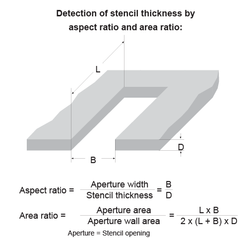
The step-upstep-down stencil is a special development for the adjustment of solder paste quantity fulfilling the needs of placement and soldering. According to IPC design guidelines 7525B there should be 89mm 035 keep-out between the step down and the aperture in the step down area for every 025mm 001 of step height. This paper is set on guidelines to minimize the process complexities and issues in production using above standard.
IPC T 50. IPC T 50. The IPC stencil guidelines are the most commonly used and are a good starting point however they do not take into account outside variables that regularly come up in all manufacturing lines such as environmental conditions oven profile printing variables squeegee pressure under-board support squeegee speed etc.
IPC-7526 Stencil and Misprinted Board Cleaning Handbook ASSOCIATION CONNECTING ELECTRONICS INDUSTRIES 3000 Lakeside Drive Suite 309S Bannockburn IL 60015-1249 Tel. This paper is set on guidelines to minimize the process complexities and issues in production using above standard. This document provides guidelines for the design and fabrication of stencils for solder paste and surface-mount adhesive.
IPC 7525A-2007 Stencil Design Guidelines This document provides guidelines for the design and fabrication of stencils for solder paste and surface-mount adhesive. Download IPC 7525A pdf. Stencil Design Guidelines 1 PURPOSE This document provides guides for the design and fabrica- tion of stencils for solder paste and surface-mount adhe- sive.
This includes differences for tin lead and lead-free solder paste overprint two-print and step stencil designs. Stencil Design Guidelines This standard establishes the guidelines for the design and fabrication of stencils for solder paste and surface mount adhesive with discussion on through-hole mixed technology and includes the differences for tin lead and lead-free solder paste overprint two-print and step stencil designs. IPC 7525A Stencil Design Guidelines Association Connecting Electronics Industries 01-Feb-2007 28 pages More details PDF AVAILABLE FORMATS IMMEDIATE DOWNLOAD 1980 4500 price reduced by 56 Quantity.
PDF AVAILABLE FORMATS IMMEDIATE DOWNLOAD 3825. More info This document provides guidelines for the design and fabrication of stencils for solder paste and surface mount adhesive with discussion on through-hole and mixed technology. One of the.
TERMS AND DEFINITIONS FOR INTERCONNECTING AND PACKAGING ELECTRONIC CIRCUITS. Much of the content is based on the experience of stencil designers fabricators and users. INTRODUCTION reduction is typically 12 Industries are focusing on reducing the overhead cost where in-house soldering defects and rework cost in surface mount device SMD assembly plays a major contribution.
During the initial Stage of Stencil design it is imperative to arrest these problems. Stencil design for various surface-mount technology as well as mixed technology with through-hole or flip chip components is discussed. It is intended as a guideline only.
Normally there is not sufficient spacing on many SMT assemblies having very small components and normal SMT components to allow this much keep-out. SMTA Chennai 30th May Optimizing SMT stencil design based on PCB layout. STENCIL AND MISPRINTED BOARD CLEANING HANDBOOK.
Applicable for Leaded SMD PiINTRODUCTION. 11 Terms and Definitions All terms and definitions used throughout this handbook are in compliance with IPC-T-50. Foil thickness Design guidelines for steps include a maximum defects like mid-chip solder balls are offered.
Printing performance depends on many different. Much of the content is based on the experience of stencil designers fabricators and users. DESIGN AND ASSEMBLY PROCESS IMPLEMENTATION FOR BOTTOM TERMINATION COMPONENTS.
5700 price reduced by 56 Quantity. The ideas and formulas mention in this document base on suggestion and analysis of these two standards above. Stencil Design Guidelines 1 PURPOSE This document provides guides for the design and fabrica-tion of stencils for solder paste and surface-mount adhe-sive.
Design of Stencil should comply with IPC-7525A. It is intended as a guideline only. GENERIC STANDARD ON PRINTED BOARD DESIGN.
IPC-7525B Stencil Design Guidelines Developed by the Stencil Design Task Group 5-21e of the Assembly and Joining Processes Committee 5-20 of IPC Users of this publication are encouraged to participate in the development of future revisions. It is intended as a guideline only as much of the con- tent is based on the experience of stencil designers fabricators and users. 8500 price reduced by 55 Quantity.
This document provides guidance for the design and fabrication of stencils for solder paste and surface-mount adhesive.

Ipc 7525a 2007 Stencil Design Guidelines
Ipc 7525 A Stencil Design Guidelines Pdf Docer Com Ar

Ipc 7525 A Stencil Design Guidelines Pdf Docer Com Ar

Ipc 7525 A Stencil Design Guidelines Pdf Docer Com Ar

Ipc 7525 A Stencil Design Guidelines Pdf Docer Com Ar

Ipc 7528b Table Of Contents Ipc 7528b Table Of Contents Pdf Pdf4pro
Smd Stencils Design Aid Multi Circuit Boards
2
0 comments
Post a Comment